SEMINARS AND WORKSHOPS
Hands-on Workshop on IC Fabrication Processand Building Blocks of VLSIDesign
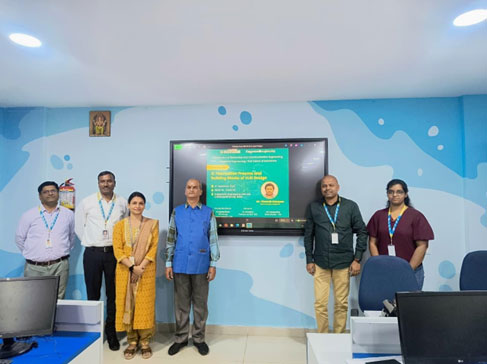
The Department of Electronics and Communication Engineering conducted a hands-on workshop on IC Fabrication Process and VLSI Design on 4th September 2025. The workshop aimed to introduce students to the fundamentals of semiconductor device fabrication and VLSI design methodologies.
Mr. Vikranth Manyam, Senior Manager at Capgemini, served as the resource person for the session. Participants were guided through essential steps of IC fabrication, including wafer preparation, lithography, doping, etching, and metallisation, along with the key challenges involved in the process.
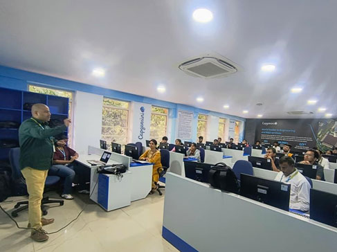
The workshop also introduced students to basic VLSI building blocks such as logic gates, flip-flops, and memory components. The hierarchical design flow from RTL to GDSII was explained, providing a clear understanding of how theoretical designs translate into physical circuits.
Hands-on activities included CAD tool demonstrations, layout simulations, and case studies that connected theoretical knowledge to practical industry applications. Students gained valuable exposure to real-world semiconductor processes and design flows, enhancing their confidence in using design tools and understanding industry expectations. Overall, the event was well-received and successfully strengthened participants’ foundations in IC fabrication and VLSI Design.