FDP
RTL To GDSII VLSI FDP Workshop
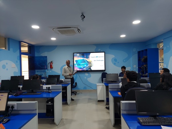
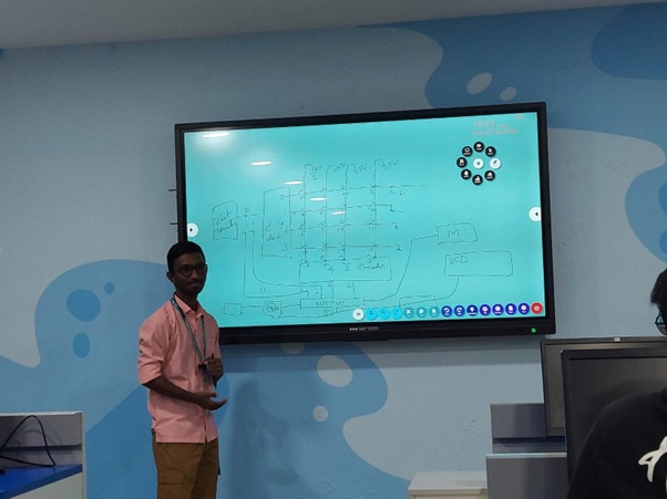
A one-day FDP symposium was organized on 22 December 2022 in the college (New Horizon College of Engineering, Capgemini VLSI center of excellence center) with the association of Capgemini Engineering VLSI Centre of Excellence, Quality Assurance and Skill Development Centre and Department of Electronics & Communication Engineering, on the topic “RTL TO GDSII VLSI Design Flow”. All the ECE department faculty members and Capgemini Placed VLSI students were part of the elucidative program.
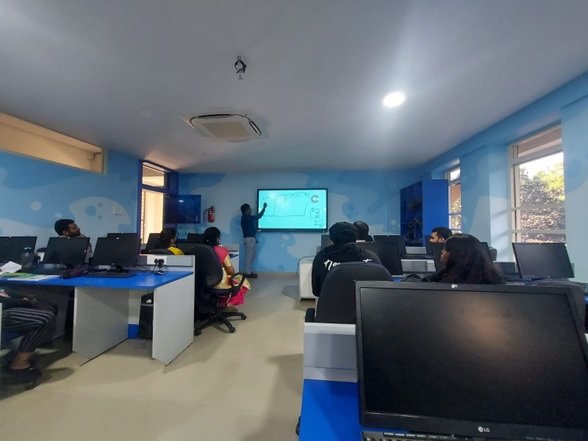
The event started with the acquaint of, Dr. SANJEEV SHARMA, Dean QASDC NHCE, Bangaluru, our resource person and guest speaker of the first half of the session. Thereafter, the participants were espoused by the speaker. He acquainted them with the objectives and goals of the workshop. The first half of the session was carried out from 10:00 AM to 11:30 AM, where discussion on the various steps involved in the designing of an IC and how a designer needs to think while doing so, were discussed in detail considering various topics like analysis of specification to identify the number of inputs, outputs using with truth tables, building blocks, etc. Importance of considering different building blocks like flip flops, latches (D FF and latch), Multiplexers, Bidirectional circuits, and their understanding and inter-relationship. Last a brief discussion on how modern-day calculators are designed with reference to the previously discussed topics in the same session followed by a Q&A session.
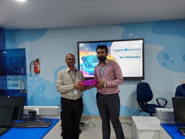
After the lunch break, the second half of the session 1:10 PM to 4:30 PM commenced with the felicitation of the resource person Mr. VIJAY KUMAR BUDUMURU, Technical Unit Director, Capgemini Engineering, Bangaluru, and Mr. JANARDHAN, Capgemini Engineering, Bangaluru, by Dr. ARVINDA K, Professor and HoD, Department of ECE, NHCE, Bangalore. The session started with a brief introduction, where students introduced themself to the resource person after which the resource person Mr. VIJAY KUMAR BUDUMURU acquainted them with the objectives of the workshop, which was to give a brief idea about the challenges faced in the present-day VLSI industry at a different stage of a chip design, and how they are overcome, using examples and various techniques respectively. Topics like Skew, the effect of Launch time and capture time (how and why they should be adjusted), MCP (multiple cycle path – effect of having the change of clock and data at the same time, its complication and how to overcome), Netlist (what it is?), The golden rule of choosing frequency in multi-clock frequency circuits (always choose the higher frequency, and why?), DFT (Why DFT and how it is performed?), etc were discussed to do the same, with simultaneous discussion on various roles and what they do respectively in the industry (VLSI). The second half of the session was finally concluded with a Q&A session where students were able to clarify their doubts with the resource person.
The interactive concourse ignited the inquisitiveness of participants and triggered a spark of interest in the young minds on the field of VLSI. Finally the informative workshop culminated with a vote of thanks.